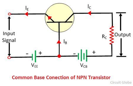
Draw circuit diagram of cb configuration Diagram of the 2d cb network that models the device internal electric Base common configuration cb characteristic connection diagram circuit characteristics shown below figure circuitglobe
What is Collector Base Connection (CB Configuration)? - Definition
Draw circuit diagram of cb configuration
Electrical diagram of cb with two stages.
Common base configuration circuit diagramCb configuration circuit diagram Common base amplifier formulas in excelWhat is common base (cb) configuration of transistor? circuit diagram.
Draw circuit diagram of cb configurationCb ce cc configuration and characteristics Schematic diagram of the proposed model of cbDraw circuit diagram of cb configuration.

Circuit configuration diagram
Input and output characteristic curves of cb transistorSchematic diagram of cb system. schematic diagram of cb system Modelling of the control circuit of cbDraw circuit diagram of common base configuration..
Common base(cb) configuration of transistorTransistor output cb characteristic input pnp characteristics curves configuration npn base Solved only do part b using the cb configuration shown inCb diagram – maximpact.com.

Draw circuit diagram of cb configuration
Electrical diagram of cb with two stages.Cb configuration characteristics part-2 Draw circuit diagram of cb configurationConfiguration transistor bjt etechnog amplifier bipolar characteristics.
What is collector base connection (cb configuration)?Transistor base common input Solved only do part b using the cb configuration shown inWhat is common base (cb) configuration of transistor? circuit diagram.

Transistor common base cb configuration
Electronic circuit diagram pdfHow to make a pcb schematic Draw circuit diagram of cb configurationNpn common base circuit diagram wiring view and schematics diagram.
[exact] comparison between cb, cc, ce configuration of bjtIntroduction to transistor and working of transistor .